Data parallelism through vector computing
Modern superscalar execution, with instruction reordering and other mechanisms to increase IPC that we have not discussed, requires complicated logic and hence a lot of power. A common case that is well suited for superscalar execution as there can be lots of independent instructions, is working with vectors and matrices. This led to the design of CPUs with instructions to work on vectors, i.e., with wider ALUs and wider registers that do not contain just a single number but a row of numbers. This has the potential to boost the speed without the full power requirements of a superscalar processor. This is one example of a single instruction stream, multiple data stream (abbreviated as SIMD) architecture.
This was a very popular design in supercomputers in the 70s and 80s, but then almost disappeared with only two or three vendors still making them (and only one still making them today). Examples are the CDC STAR-100 from 1974 and the Cray-1 from 1976. The latter was the first vector computer to use a design with registers. The STAR-100 streamed the data directly from and to memory. Currently NEC still makes vector computers though with a slightly different design as before for even faster speeds. Vector registers in the current NEX SX Aurora TSUBASA architecture are 256 double precision numbers wide, and the execution unit itself is 32 double precision numbers wide, executing a 256-number vector instruction in 8 steps.
Vector instructions are also returning in general purpose computers, but then with much shorter vector lengths.
In the Intel architecture, MMX integer vector instructions with 64-bit wide registers were introduced in 1996 and available in 1997 on an evolution of the Pentium processor. They basically re-used the floating point registers in those processors for storing integer vectors so codes could not combine floating point instructions and integer vector instructions. They were meant for media processing and not all for scientific computing. Just a few years later, in 1999, Intel launched the SSE instruction set which used separate 128-bit registers. Originally they were only meant for single precision floating point numbers (so 4 elements in a vector), and they became available in the Pentium III processor which was actually an evolution of the Pentium Pro and not of the original Pentium. The instruction set was extended several times with SSE adding double precision floating point numbers and some integer instructions in the Pentium 4, and with further extensions in the SSE3 and SSE4.x instruction sets. MMX instructions are not present anymore in modern Intel processors in 64-bit mode, but the SSE instructions are still present and were exploited in a lot of good scientific computing codes. A further extension came with the AVX instruction set in the Sandy Bridge generation in 2011. The vector registers were extended to 256 bits and could now handle 4 double precision or 8 single precision numbers simultaneously. AVX2 extended the AVX instruction set in the Haswell generation and came at the same time as the FMA3 instructions, the so-called fused multiply-add instructions that combine a multiplication and an addition in the form a*b+c, effectively doubling the number of floating point operations per clock cycle. A further evolution came in the AVX-512 instruction set using 512-bit wide vectors but also adding other features that make the vector instruction set a lot more useable (and a lot more like those on the traditional vector computers). They were first introduced in the now defunct Xeon Phi processor, a processor specifically designed for supercomputers, but got a new life in the server variant of the Skylake architecture (Skylake X) and the more recent Ice Lake and Sapphire Rapids processors. In fact, Intel keeps adding new instructions for new data formats, especially for AI where some deep learning applications can benefit from lower precision data formats. To reorganise the mess around AVX-512 and its extensions, Intel has now introduced the AVX10 instruction set.
The ARM instruction set has known the NEON vector instructions for quite a while already. These instructions use 128 bit registers, so can work on 2 double precision or 4 single precision floating point numbers. Even the processors in most mobile phones support these instructions. But the ARM architecture is also evolving. ARM designed the SVE instruction set (Scalable Vector Extension) together with Fujitsu for use in supercomputers. SVE instructions allow for different implementations with vector registers up to 2048 bit wide, which can store 32 single precision or 64 double precision numbers, but also supports implementations with registers as small as 128 bits. The implementation of Fujitsu which is used in the A64fx processor of the Fugaku supercomputer (which was the fastest machine in the Top500 lists from June 2020 till November 2021) uses 512-bit registers. These instructions have been extended with SVE2 instructions that are more oriented towards integer computations and making the instruction set more useful for non-scientific applications. SVE2 is now part of the new ARMv9 architecture and used in, e.g., the processors of the Samsung S22 and newer high-end S-series mobile phones, the Apple A18 processor uses in the iPhone 16 series and the Apple M4 processor used in various Mac models and some iPads, but also in the NVIDIA Grace CPU that are used in the GPU-accelerated nodes of the first European exascale supercomputer and are also used in the GPU-accelerated nodes of the Swiss Alps supercomputer operated by CSCS.
AMD also uses vector units int its GCN and CDNA GPUS, with 16-wide single precision hardware and 64-wide single precision instructions (well, not completely true for CDNA2), and in its RDNA GPUs, with 32-wide single precision hardware and instructions. The Intel GPUs are also based on vector computing units with 8-wide units for most basic operations.
Vector instructions in VSC clusters
The Intel Sandy Bridge processors, the ones to introduce the AVX instruction set, were also used in the first Tier-1 cluster of the Vlaams Supercomputer Centrum, installed in 2012, and in the hopper cluster of the University of Antwerp.
AVX2 was really popular, even when AVX-512 was already around, as AMD only adopted AVX-512 in their 4th generation EPYC CPUs code named Genoa, and as Intel has never really adopted the instruction set in the PC space. The University of Antwerp cluster Leibniz used the intel CPUs code name Broadwell, as did the older section of the second VSC tier-1 computer, BrENIAC. Vaughan and the third VSC tier-1 computer use 2nd and 3rd gen EPYC CPUs code named Rome and Milan respectively which also provide the AVX2 and FMA3 instructions.
AVX-512 appeared in Intel Skylake and later generations, and in AMD EPYC Zen4 CPUs (code named Genoa) and later. Skylake and later generation Intel CPUs can be found in the VUB Hydra compute service, the Intel-based partitions of the UGent clusters and the KU Leuven Genious and wICE clusters. The VUB Hydra cluster also has a number of nodes with AMD Zen4 CPUs.
One step further: Matrix instructions
It hasn't stopped with vector instructions. To support AI inference, GPUs have introduced matrix instructions, basically matrix multiplication, though often only for low-precision data formats though the AMD CDNA2 an later variants of this architecture also have them for single (FP32) and double (FP64) precision data formats.
These also are starting to make their way into CPUs. Intel has already defined the AMX instruction set of low-precision matrix operations, implemented in some of their server CPUs. IBM introduced the MMA (Matrix-Multiply Assist) instructions in POWER10. And the ARM v9.2 instruction set introduced the optional Arm Scalable Matrix Extension (SME) instruction set extension.
Another type of SIMD computing
There is however another way to reduce the overhead of superscalar execution that works well for vector operations.
Rather than widening the ALUs and registers, we can also just use multiple sets of ALU, register and AGU/load-store units, but use only a single control unit so that all those ALU-register-AGU combinations have to execute the same instruction at the same time, or do nothing, but of course can operate on different data.
This design is shown in the following figure:
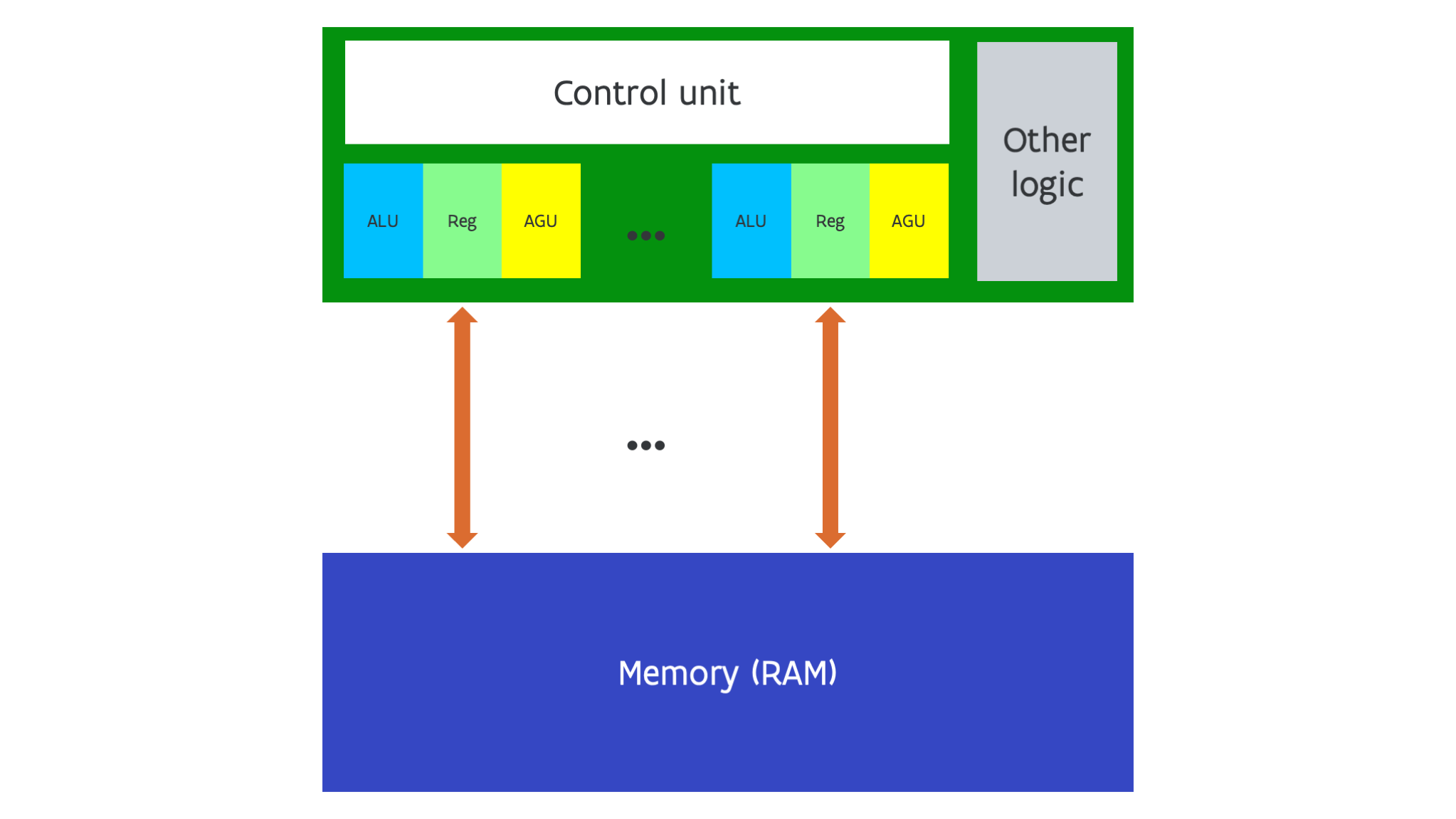
The historical example of this design is the Thinking Machines connection machine with the first generation CM-1 machine launched in 1983. However, NVIDIA GPUs are a modern example of this design combining 10s or even 100 of those SIMD processor (which they call SIMT processor) on a chip.
Such processors may seen easy to program as it looks as if you can think in terms of scalar operations rather than vector operations, but in reality it is not easier to program them efficiently that it is to program vector machines. And NVIDIA may claim otherwise, but there is little difference in what the processors can do between this form of SIMD computing and a vector computer with an instruction set that also supports so-called masking or prediction and scatter-gather operations. Which is in fact also the difference between the AVX-512 and AVX2 instruction sets.
Conclusion on intra-processor parallelism
There are two levels of parallelism in modern processors:
-
Trying to execute more instructions per clock cycle: instruction-level parallelism, abbreviated ILP.
This is mostly hard work for the CPU control logic and for the compiler, and only a limited amount of work for the application developer. Moreover, you can expect a gain from this technology even without recompiling your application for a newer CPU if that CPU supports the same instruction set.
-
Doing more work per instruction: data-level parallelism through vectorisation or other SIMD technologies
This is a much harder job for the compiler as most programming languages do not offer enough information to the compiler. The application developer often needs to help the compiler.
Moreover, you will not gain from the addition of vector instructions to a processor design without recompiling for those vector instructions.
In some applications a lot of the gain over the various generations of CPUs since the late '90s has come from better and wider vector instruction sets. But these improvements can only be delivered if an application gets recompiled for those new instructions (and then it won't run anymore on the older processors). This is one of the reasons reason why on supercomputers applications are often installed from source code rather than from binaries.