The memory pyramid
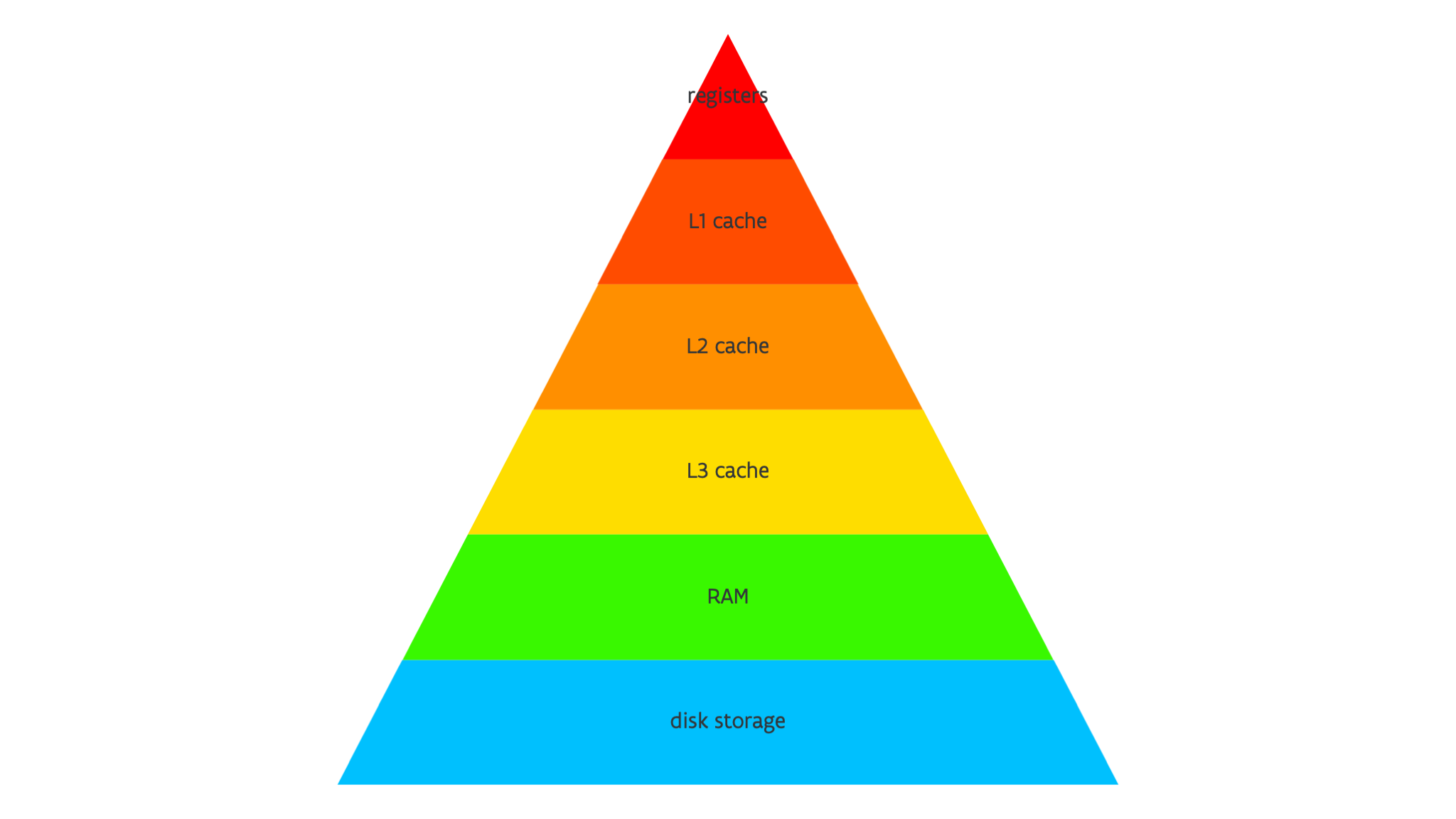
We've seen several types of memory now, and that is structured in a hierarchy. The typical hierarchy for a regular CPu is depicted above.
-
Each core has registers for integer data, floating point data and/or vectors, and some special registers. The architectural register set is rather small but as this limits parallel execution inside the processor, modern processors have a lot of hidden register space that is used through an automatic mechanism called "register renaming". E.g., the AMD Rome or Milan processors have less than 1 kB of register space in the instruction set, but the total physical register space (used with register renaming) is over 6 kB.
-
Processors typically have separate L1 caches for instructions and for data (where the data one is sometimes bypassed when using vector instructions).
-
The L2 cache in processors for scientific computing is typically on a per core basis.
-
The L3 cache is shared by a number of cores, sometimes even by all cores in a socket
-
The next level in the hierarchy is the main RAM memory, which due to the NUMA architecture may appear as multiple levels with different latency and bandwidth
-
The last level is one that will actually be de-activated on many supercomputers as it is too slow: When RAM memory is exhausted, the OS can swap some of the content to disk storage. But even without swapping enabled we can still see the disk as an additional storage space, but then one that we need to manage ourselves in software.
Some supercomputers will offer several types of disk storage. Typically a smaller volume based on SSD technology and a slower but larger volume based on regular hard disks.
Even this picture is still oversimplified. Processors have other types of small caches, but those are harder to exploit by our programming style so we should not really take them into account here. RAM memory may also exist out of multiple layers instead of the one depicted in the picture.
-
The Intel Xeon Max 9xxx series has 64 GB of high-bandwidth RAM on each socket and then up to 1 TB or more of lower bandwidth memory connected externally to the socket.
This chip is used in a small subsection of the EuroHPC pre-exascale system MareNostrum 5 (and were planned for the pre-exascale system Leonardo).
-
Recently for large memory computers, and especially for database systems, a new type of RAM package was proposed that is connected to an expansion card on the CXL-bus, an evolution of the PCIe bus (and IBM has its own alternative in its CPUs). Obviously this memory sits even further away from the CPU so we can expect a higher latency and less bandwidth. Given that scientific computing applications are often already memory latency and/or memory bandwidth limited, this memory type may never become very useful in supercomputers.
Let us compare the memory hierarchy for the "Leibniz" cluster and AMD Rome section of Vaughan of the UAntwerpen infrastructure for 2023, and then with Hawk, one of the largest CPU-only systems in Europe, at HLRS in Germany, and also based on the AMD Rome CPU
| Leibniz "Broadwell" | Vaughan "Rome" | Hawk "Rome" | |
|---|---|---|---|
| architectural registers | <1 kiB/HW thread | <1 kiB/HW thread | <1 kiB/HW thread |
| physical registers | ~7 kiB | ~6 kiB | ~6 kiB |
| L1 cache | 2 x 32 kiB/core (I+D) | 2 x 32 kiB/core (I+D) | 2 x 32 kiB/core (I+D) |
| L2 cache | 256 kiB/core | 512 kiB/core | 512 kiB/core |
| L3 cache | 35 MiB/socket | 128 MiB/socket | 256 MiB/socket |
| L3 organization | 35 MiB/socket | 16 MiB / 4 cores | 16 MiB / 4 cores |
| RAM | 128 or 256 GiB/node | 256 GiB/node | 256 GiB/node |
| disk swap | disabled | disabled | disabled |
| disk storage | 600 TB | 600 TB | 26 PB |
| size cluster | 152 nodes | 152 nodes | 5632 nodes |
So we see that there is in fact very little difference in the hierarchy for a university level supercomputer as Leibniz and Vaughan and a very large national or international supercomputer. However, the total size is very different.